EEVblog #532 - Silicon Chip Wafer Fab Mailbag
A look at some equipment and wafers used in the manufacture of silicon chip wafers.
200mm and 300mm wafers, die, dice sawing, lead-frame manufacture, automated testing machine (ATE) probing, clean room bunnie suits, photo plots, BGA chip thermal test sockets, and the worlds smallest active FET probes at 100 nanometers for direct wafer probing!
Thanks to Vincent Himpe:
/
Forum: /
EEVblog Main Web Site:
EEVblog Amazon Store:
Donations:
/
Projects:
/
Electronics Info Wiki:
/
Rcreviews.lt is not the owner of this text/video/image/photo content, the real source of content is Youtube.com and user declared in this page publication as Youtube.com user,
if you have any question about video removal, what was shared by open community, please contact Youtube.com directly or report bad/not working video links directly to video owner on Youtube.com. Removed video from Youtube.com will also be removed from here.
Watch more videos
-
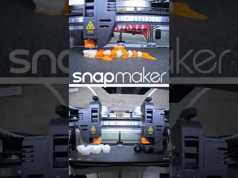 SnapMaker J1 IDEX 3d printer - double extruder workflow sample dual head print
#shorts Enjoy double extruder workflow satisfaction Music by: Gibran Alcocer - Idea 1 - piano c... -
 #DriftMolėtai "Street" drift race finals 2022
Happy drift day! Had a chance to be part of Moletai street drift race Finals! #DriftMolėtai grį... -
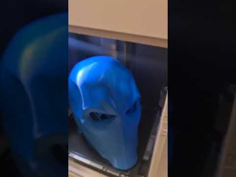 DeathStroke BambuLab X1C #Shorts
#shorts DeathStoke wearable mask made with BambuLab X1C #3dprinting


Advertising